14 June 2026
The STM32C031C6 Nucleo 64 board features a SWD interface, and no JTAG interface. Regardless of which debugging probe is used, it is this SWD interface that will be used. There are multiple ways to connect to this interface, and each requires the proper configuration of jumpers and/or connections to exposed header pins.
Like all Nucleo 64 boards, it comes with an on-board STLink debug probe (specifically the STLinkV2-1). This means there are two main cases to consider when debugging the target.
As previously noted, regardless of which case, each connects to the SWD pins on the target, the only difference is in how this is accomplished. In order to keep this write-up on topic we will simply go over the necessary connections for each case and keep the explanations brief. We hope to have more detailed guides going into the details later, including looking at the schematic to understand more about why certain connections are made.
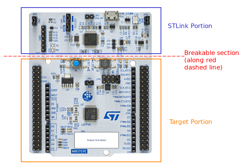
First, we do need to go over certain parts of the board that are key to configuring the setup. There are two main portions of the board as shown below, separated by large cut-out areas, with small pieces connecting them. These portions are the STLink portion and the Target portion (the target portion contains the main STM32C031C6).
In addition to knowing the portions, there are several key components distributed between the two portions in the form of headers and jumpers.
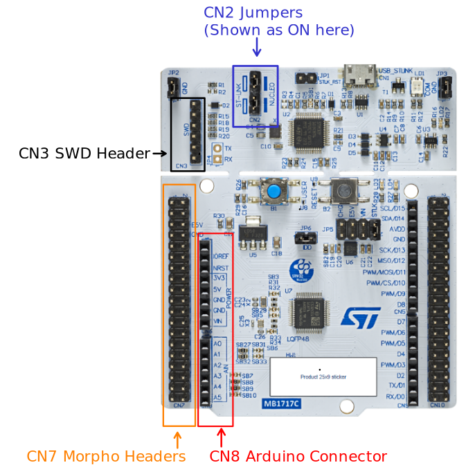
In list form:
If the STLink portion of the board is removed by the user (by snapping along the green line shown in the first image) we lose access to CN2 and CN3.
One last thing to note is which pins on the CN7 Morpho header correspond to SWD pins since these cannot be used when using them for SWD debugging. There These are shown below. Note the 3v3 pins can be used, they’re just voltage supplies. It is the PA13, PA13, PF2 that cannot be used.
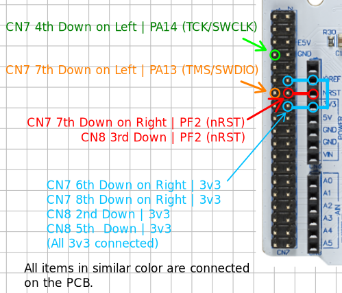
Note, the holes in the CN8 header are hard to see, but there is one on top that is not labelled, and the second one below it is where the labelling starts with the IOREF, and the third being NRST which is where the typical Arduino header starts (with reset).
Without going into too much detail using the schematic, the relationship between the headers and jumpers is shown below. Note the 3v3/IOREF annotations are removed to make it slightly less of a mess.
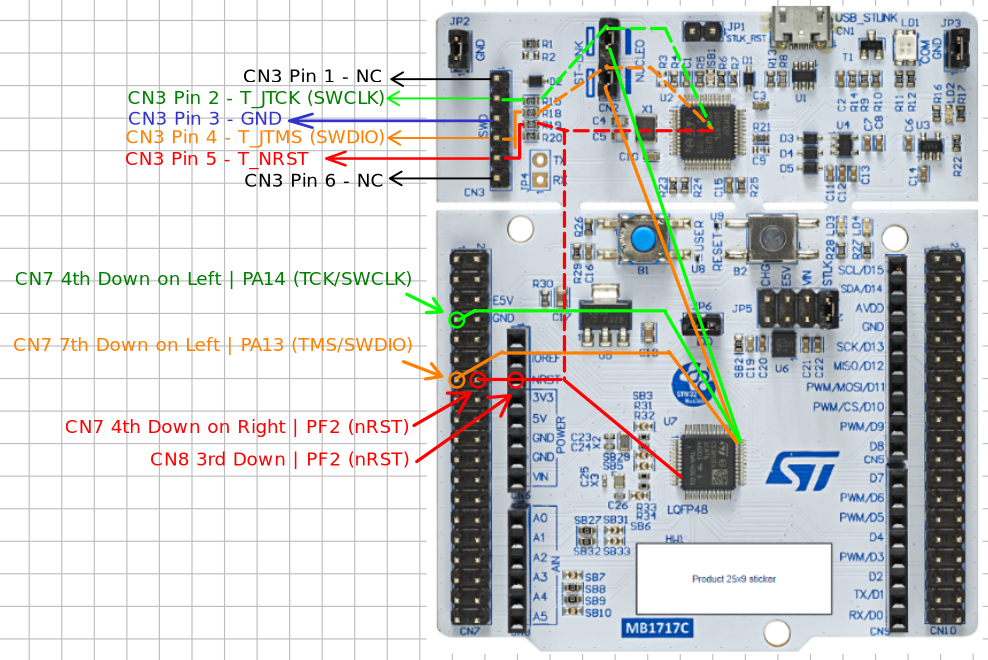
Note:
Also note:
The most important thing to realise here is the CN3 connector is connected to the STLink regardless of jumper configuration, and that CN2 is used to connect the STLink to the STM32C031C6.
As noted above in the jumper section, with the jumpers connected the STLink is directly connected to the SWD lines for the target. After this STLink simply needs to be connected to using the USB connector and it will be available for debugging.
To connect an external debugger we have two cases:
Realistically, only one configuration is needed that will work in both cases, and uses the Morpho pins on the target portion of the board. However, it is also possible to use the CN3 header though the only real reason for doing so is for a more “elegant” looking connection. By that I mean you will have a nice sequence of jumpers connected to the CN3 header rather than a rat’s nest on the Morpho headers.
So, rather than grouping the connections based on the presence of the STLink, we’ll simply group them based on which headers are used, and then list what situations they cover. The options then are:
Works for cases:
The most foolproof connection involves using the CN7 Morpho header pins since it doesn’t matter if the STLink is connected and doesn’t require jumper configuration.
To use this, simply connect your debug probe to the appropriate pins. One such configuration is:
Note, when looking at the board from the top, with the STLink portion on top, the CN7 pin numbers start with 1 on the top left and zig zag down like so:
                      CN7 Pinout
                      =========
                     | 1  | 2  |
                     | 3  | 4  |
                     | 5  | 6  |
(PA14 TCK/SWCLK) --- | 7  | 8  | --- (GND)
                     | 9  | 10 |
                     | 11 | 12 | --- (3v3/IOREF)
(PA13 TMS/SWDIO) --- | 13 | 14 | --- (PF2 nRST)
                     | 15 | 16 | --- (3v3/IOREF)
                     | 17 | 18 |
           (GND) --- | 19 | 20 |
                     | 21 | 22 |
                     | 23 | 24 |
                     | 25 | 26 |
                     | 27 | 28 |
                     | 29 | 30 |
                     | 31 | 32 |
                     | 33 | 34 |
                     | 35 | 36 |
                     | 37 | 38 |
                      =========

         Debug Probe Pin  |  CN7 Pin
         ---------------- | ---------
                    GND   |   8 or 19
                   Vref   |   12 or 16
                  SWDIO   |   13
                  SWCLK   |   7
                   nRST   |   14
---------------- | ---------As noted above, if one wants a more “elegant” looking connection, it is possible to use a combination of the Morpho CN7 Header and the CN3 Header. In this case the CN3 header is used for most SWD connections, but the CN7 header is still used for the reference voltage connection.
                      CN3 Pinout
                         ===
                        | 1 |
            TCK/SWCLK   | 2 |
                  GND   | 3 |
             MS/SWDIO   | 4 |
                 nRST   | 5 |
                        | 6 |
                         ===

========================================================

                      CN7 Pinout
                      =========
                     | 1  | 2  |
                     | 3  | 4  |
                     | 5  | 6  |
(PA14 TCK/SWCLK) --- | 7  | 8  | --- (GND)
                     | 9  | 10 |
                     | 11 | 12 | --- (3v3/IOREF)
(PA13 TMS/SWDIO) --- | 13 | 14 | --- (PF2 nRST)
                     | 15 | 16 | --- (3v3/IOREF)
                     | 17 | 18 |
           (GND) --- | 19 | 20 |
                     | 21 | 22 |
                     | 23 | 24 |
                     | 25 | 26 |
                     | 27 | 28 |
                     | 29 | 30 |
                     | 31 | 32 |
                     | 33 | 34 |
                     | 35 | 36 |
                     | 37 | 38 |
                      =========

========================================================

         Debug Probe Pin  |  CN3 Pin
         ---------------- | ---------
                    GND   |   3
                  SWDIO   |   4
                  SWCLK   |   2
                   nRST   |   5
         ---------------- | ---------

========================================================

         Debug Probe Pin  |  CN7 Pin
         ---------------- | ---------
                   Vref   |   12 or 16
         ---------------- | ---------